NICMOS 3 Focal Plane Array Technical Description
The focal plane array (FPA) consists of a HgCdTe
detector array hybridized to a silicon multiplexer using indium columns
(bumps). The detector array converts the incoming infrared radiation into
electrical charge and the multiplexer processes the charge. The two
components
are fabricated separately, resulting in the independent optimization of the
performance of each device. Indium columns are evaporated on the detector
and multiplexer array after each is fabricated.
The two devices are then aligned
and cold-welded together to form the hybrid focal plane array. The hybrid is
illuminated through the substrate--in this case, sapphire.
The key component of the hybrid FPA is the
readout multiplexer, which converts the integrated detector current into an
output voltage and multiplexes the detectors into a serial data stream. The
multiplexer was designed using 3-micron, single polysilicon, single metal,
p-well
CMOS design rules. The multipexer circuit consists of an array of MOSFET
switches arranged so that each detector element is read out through a single
unit
cell repeated as a 128x128 array, connecting to each detector
through an indium
column. Four such arrays are mosaiced to form the NICMOS 3 256x256 detector.
The detector is biased to a voltage VR - DetSub.
In our case, this is a reverse
bias level of 0.5 volts. After the detector is read, the reset switch is
turned on,
forcing the potential at the cathode of the detector to voltage VR.
When this
switch is then opened, the cathode of the detector is free to float in
potential.
Each detector has a depletion capacitance into which the photogenerated and
leakage currents are integrated. As charge integrates, this potential
discharges
toward DetSub. LIRC-II uses the reset gate for each pixel so that correlated
double sampling can be used to reduce kTC noise. For correlated triple
sampling
and multiple readout of the same exposure, the reset gate is not used. This
software-controllable feature is not yet an option in the LIRC-II camera
system.
Unfortunately, the process of resetting the detector bias is not uniform.
This
shows up as a non-uniform DC offset in the output signal. This is due to
threshold variations caused by non-uniformity in the silicon MUX and
processing variations. Because these non-uniformities are the result of
materials
variations, and not random electrical noise, they are repeatable from one
readout
of the array to the next and can therefore be removed by calibration.
The array uniformity is determined by the uniformity of the MUX and the
detector material. Due to the way the MUX is laid out, there is a systematic
odd/even offset built into the MUX. This offset is removed by most sampling
schemes or by simple flat field calibration.
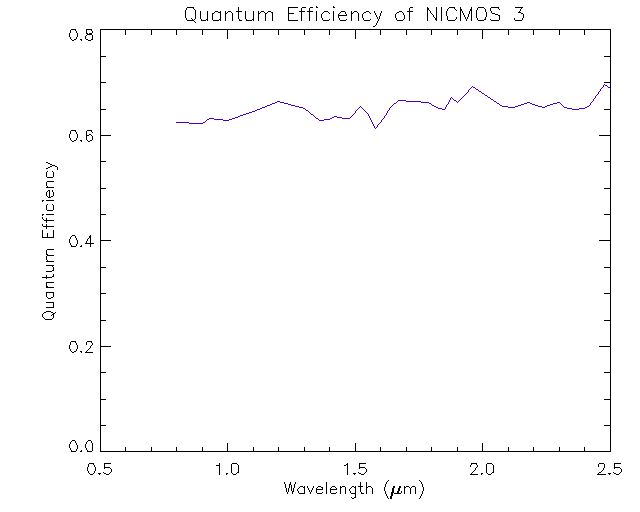
Array Quantum Efficiency
The following QE curve is for the IRIM camera at KPNO, but should be reasonably close
to the curve for LIRC II.